SMD (surface mount device) sensors have been specifically designed for fully automated placement on PCB’s (printed circuit boards). Billions are produced each year and they are now the most widely used resistor on PCB’s. There are a number of reasons for this trend, including the following::
- low cost
- placement automation
- improved miniaturization
- interchangeability
- durability
The fact that SMD’s can be handled via pick and place machines is a significant advantage of this type of sensor. This automation means that high volume production is possible and minimal manual labour is required (contributing to the low cost).
SMD sensor components are mounted onto PCB’s using “surface mount technology” (SMT). In the first step of manufacture, a pick and place machine removes the SMD component from a roll of blister packs and places it on the top and/or bottom of a PCB. In the second step automatic soldering of the component takes place using wave, reflow or vapour phase.
With regards to miniaturization, there is a growing trend in new electronic designs towards the smallest possible component-PCB packages with which power dissipation is still possible. SMD’s match this trend which saves board space and provides more functionality in the same amount of space.
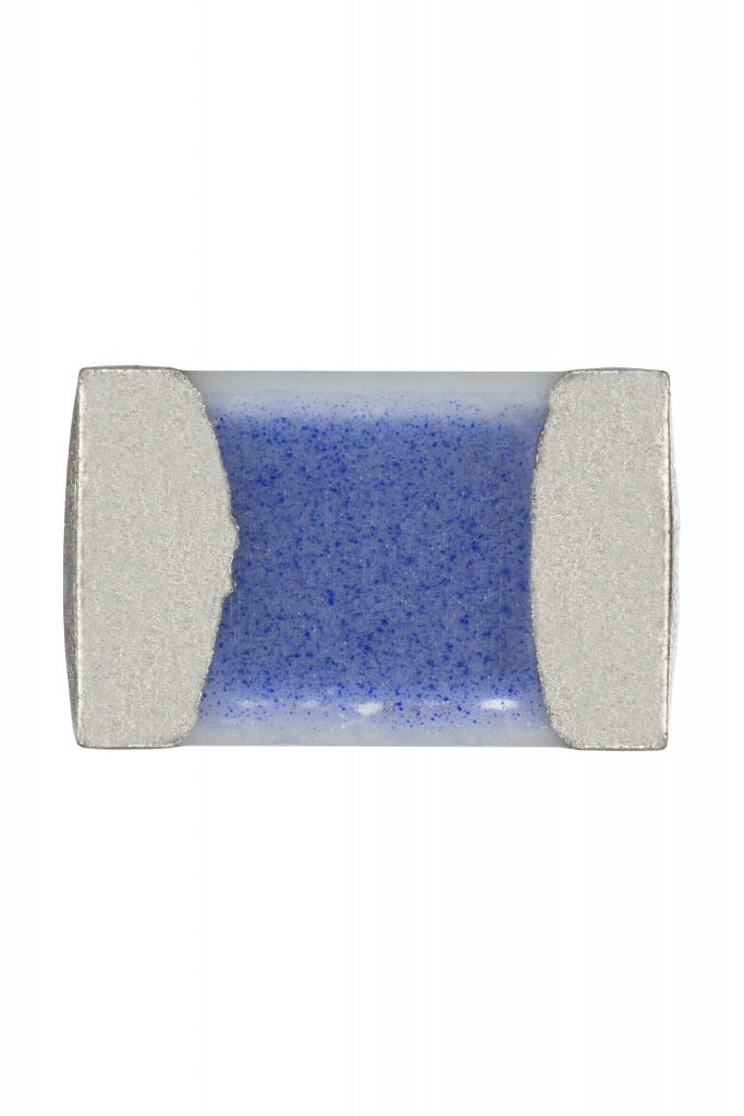
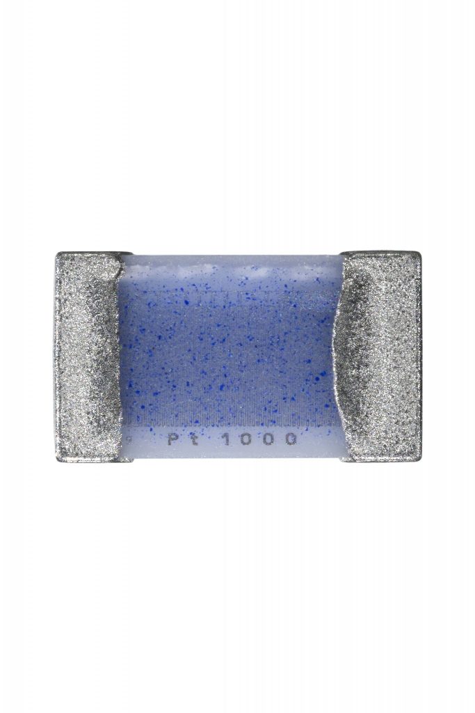
The durability of SMD’s depends on the type used, for example an NTC SMD can withstand mechanical stresses very well. However, Pt SMD’s have the advantage of a higher temperature tolerance as well as layers of protective coating ensuring protection from corrosion, oxidation etc. Long term resistance stability is another aspect of the durability of SMD’s.
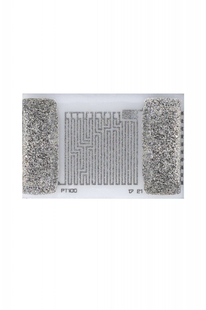
Another advantage of using SMD’s on PCB’s is that they can be designed to reduce the thermal impact of the wire temperature on the sensor elements. This is achieved by using a meander conductor path to connect the sensor element and the soldering pads. The PCB itself separates the soldering wires into front and back which reduces the risk of a shortcut.
In general, SMD’s have much lower levels of stray inductance and can therefore be used for much higher frequency operations. They can be manufactured to high tolerances and have excellent accuracy.
Using SMD’s removes the need for lead wires such as are required with the older ‘through hole technology’. Through hole technology also requires manual fitting of components and (expensive) drilling of holes in the PCB. In general SMD’s are chosen for most manufacturing processes because of it being so much more cost-effective.
Through hole technologies are better for components that will be under stress or for the quick production of prototypes.
Please contact our team of specialists for any questions you might have about SMD sensor design, choice and the particular products offered by Kamet. You can read more about SMD’s in general on our product page and you can also choose to request a quote via our contact page.